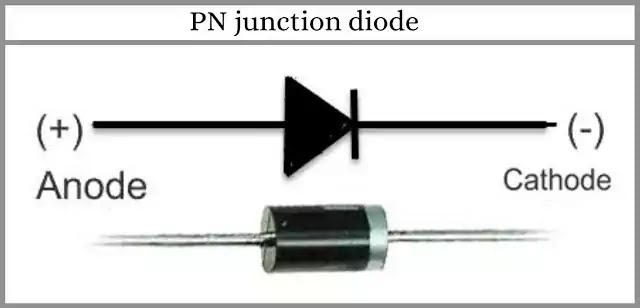
What is a PN Junction Diode ?
The PN Junction diode is a semiconductor device that is a combination of n-type and p-type semiconductor materials which are usually made of silicon or germanium. The n-type is always negatively doped and has electrons as its majority charge carriers and the p-type is always positively doped and has holes as its majority charge carriers.
What do we mean by positively or negatively doped, Doping is a technique that adds impurities into the materials so that excess holes or electrons can be made in materials. Without doping there will be free electrons or holes which makes the semiconductor materials like silicon useless in their original form.
The making of excess holes is said to be positively doped and it is usually done with the materials like boron or gallium injected in the p-side and the making of excess electrons is said to be negatively doped and is usually done with the materials like arsenic or phosphorus injected in the n-side.
Working of PN Junction Diode
We know that the PN junction is formed by combining the n-type and p-type semiconductor materials. These materials are doped negatively and positively respectively. Due to doping, there are excess electrons and donor ions on the n-side and there are excess holes and acceptor ions on the p-side. The free electrons from the n-side start diffusing towards the p-side and combine with the holes and the acceptor and donor ions are left alone. These ions become immobile and form the depletion layer.
This layer has both positive and negative ions that are immobile and they also contain few charge carriers that are thermally generated in this depletion region. These ions create an electric field and point from the positive ions to negative ions in this depletion region. An electric field that flows from the positive ions to the negative ions in the depletion layer creates a potential barrier that restricts the further flow of electrons from the n-side to the p-side. The synonymy for the potential barrier discussed here is built-in potential.
Now the PN Junction has the following three biasing conditions they are:
Zero Biased
This condition revolves around the idea of not applying the bias that io external voltage is given to the diode. The pure diode without any external electrical or voltage supply is the zero-biased PN Junction diode. This keeps the diode in a state of equilibrium.
Forward Biased
Forward biasing refers to the type of biasing that involves connecting the external voltage in such a way that the positive terminal is connected to the p-side and the negative terminal is connected to the n-side. This brings the potential that helps the good amount of charge carriers towards the PN junction. This leads to a decrease in the size of the depletion layer and causes the derailment from a state of equilibrium.
Reverse Biased
Reverse biasing is just opposite to forward biasing and involves connecting the negative terminal of an external voltage to the p-side and the positive terminal to the n-side. This leads to an increase in the size of the depletion layer. So the potential barrier also rises and the diode acts as a resistor in this condition as no current flows.